Both glass-based and film-based sensors are evolving to improve performance, while at the same time becoming thinner and lighter, and increasing optical quality, according to new data from NPD DisplaySearch (www.displaysearch.com).
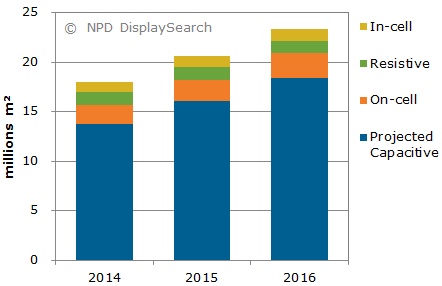
The research group forecasts that the total touch sensor area yield of projective capacitive, in-cell, on-cell, and resistive sensors, will reach 23.3 million square meters in 2015, up from 18 million square meters in 2014. Capacity for sensors for film substrates will be higher than for glass substrate, due to expected area growth of each type of film structure.
“Metal mesh, sliver nanowires, and other new materials will be used in the production of larger displays with better sheet resistance at affordable prices, and these new materials might be used for curved or flexible-touch sensors soon,” says Shoko Oi, deputy director of touch panel and emerging display research for NPD DisplaySearch.
Taiwan will continue to be the top region for manufacturing touch sensors through 2016. However, due to strong demand from local smartphone and tablet PC brands, China is expected to rise to #2 in 2016, according to NPD DisplaySearch.
